Boffins develop radically new camera sensor... that Sigma tried 20 YEARS ago!
Could the essence of the Foveon X3 image sensor be due a come-back? Swiss scientists seem to think so
The best camera deals, reviews, product advice, and unmissable photography news, direct to your inbox!
You are now subscribed
Your newsletter sign-up was successful
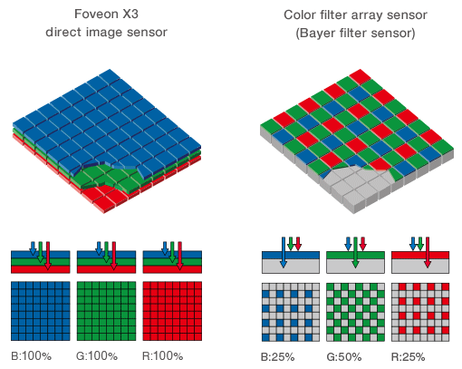
Photographic image sensors are continually evolving, with technologies like stacked sensors, pixel binning and RYYB sensor arrays all touted as having improved image quality to some extent. However, all these advances have essentially been tweaks of the same Bayer sensor formula, which arranges the red, green and blue elements of a sensor's pixels adjacent to each other in a grid formation. Then a color filtration layer above the pixels ensures each R/G/B photodiode only absorbs the light wavelength it's supposed to.
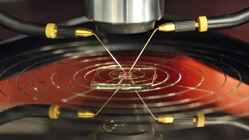
But while billions of Bayer-based image sensors have now been produced, that hasn't stopped a group trying to develop an entirely new image sensor design that addresses the flaws of the Bayer pixel layout. The consortium comprises Maksym Kovalenko from Thin Films and Photovoltaics laboratory (a sub-department of Empa - the Swiss Federal Laboratories for Materials Science and Technology), Ivan Shorubalko from Empa's Transport at Nanoscale Interfaces laboratory, as well as ETH Zurich researchers Taekwang Jang and Sergii Yakunin. The secret to the new sensor's construction is the material the snesor is actually constructed from. A traditional Bayer sensor is made from silicone, however the new sensor uses a mineral compound called perovskite - a calcium titanium oxide material.
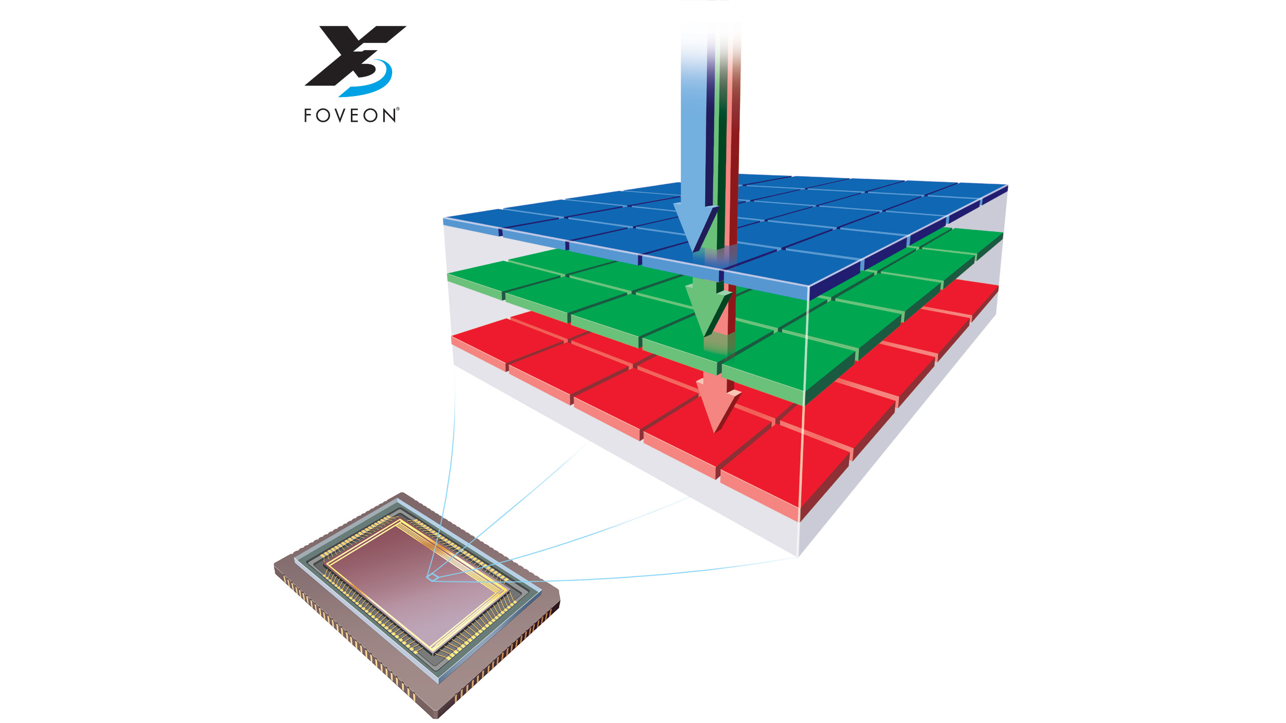
The advantage with using perovskite over silicon is that you can do away with the color filter layer of a Bayer sensor, and thereby increase light transmission to the pixels. This is due to the color filtration essentially being already 'built into' the perovskite material - researchers have managed to produce perovskites (specifically those of the lead halide variety) which only absorb light of a certain wavelength and are transparent to other wavelengths. This means that the pixels for red, green and blue can be stacked on top of each other instead of being arranged next to each other. Consequently, by stacking the red, green and blue pixels, the sensor can capture around 3x more light than a Bayer sensor of equivalent dimensions - a potentially huge gain for boosting dynamic range and reducing image noise.
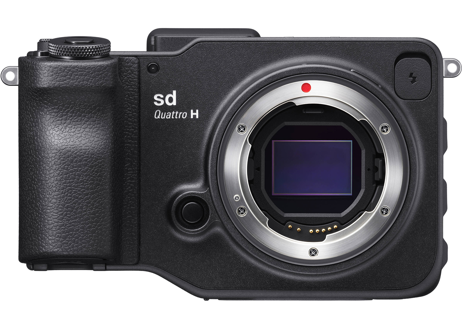
Article continues belowIf all this sounds somewhat familiar, you're not wrong. The Sigma Foveon X3 image sensor was another radically new sensor design that debuted back in 2002 but never gained widespread popularity. It too used a stacked R/G/B sensor construction, also promising the same kind of light transmission gains as the new perovskite-based sensor.
So will we see perovskite sensors in a camera or camera phone any time soon? Probably not. As with any new technology, there are challenges to be overcome. Firstly, the concept has only currently been proven with a basic sensor construction containing pixels up to five millimetres in size. The challenge now is to miniaturize a perovskite sensor so it can contain the kind of megapixel counts we've now come to expect from a conventional image sensor. Perovskite is also more sensitive to environmental influences than silicon, requiring new manufacturing processes. However on the upside, perovskite is said to be less sensitive to material defects.
Story credit: Chem Europe
The best camera deals, reviews, product advice, and unmissable photography news, direct to your inbox!
Ben is the Imaging Labs manager, responsible for all the testing on Digital Camera World and across the entire photography portfolio at Future. Whether he's in the lab testing the sharpness of new lenses, the resolution of the latest image sensors, the zoom range of monster bridge cameras or even the latest camera phones, Ben is our go-to guy for technical insight. He's also the team's man-at-arms when it comes to camera bags, filters, memory cards, and all manner of camera accessories – his lab is a bit like the Batcave of photography! With years of experience trialling and testing kit, he's a human encyclopedia of benchmarks when it comes to recommending the best buys.
