Sony is about to debut a potentially game-changing new image sensor
The new Sony Xperia 1 V flagship phone is coming, and it looks like it'll be packing fundamentally new camera tech

The best camera deals, reviews, product advice, and unmissable photography news, direct to your inbox!
You are now subscribed
Your newsletter sign-up was successful
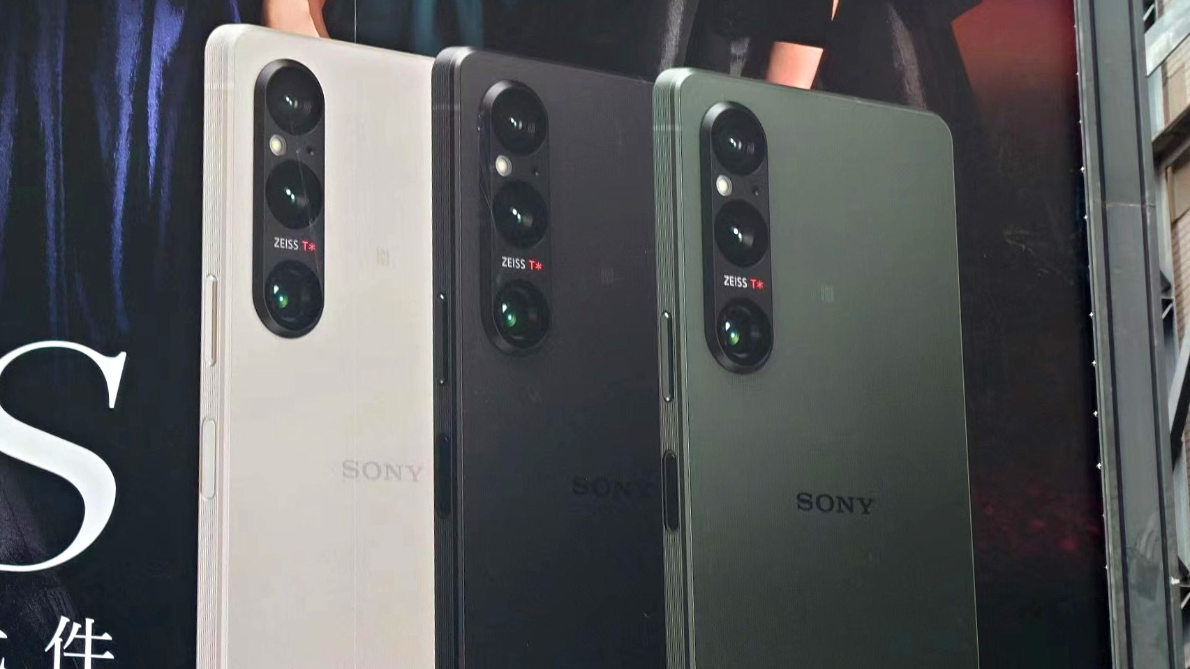
The Sony Xperia 1 V is about to launch on May 11, and according to advertising in Hong Kong, it'll feature a brand new type of image sensor. Refreshingly, we're not just talking about an even higher megapixel count, or a slightly larger sensor size, but rather a whole new CMOS sensor architecture.
The new 'dual-layer' sensor technology, developed by Sony, was originally unveiled back in late 2021, but the Xperia 1 V looks like it will be the first commercial implementation of this type of sensor.
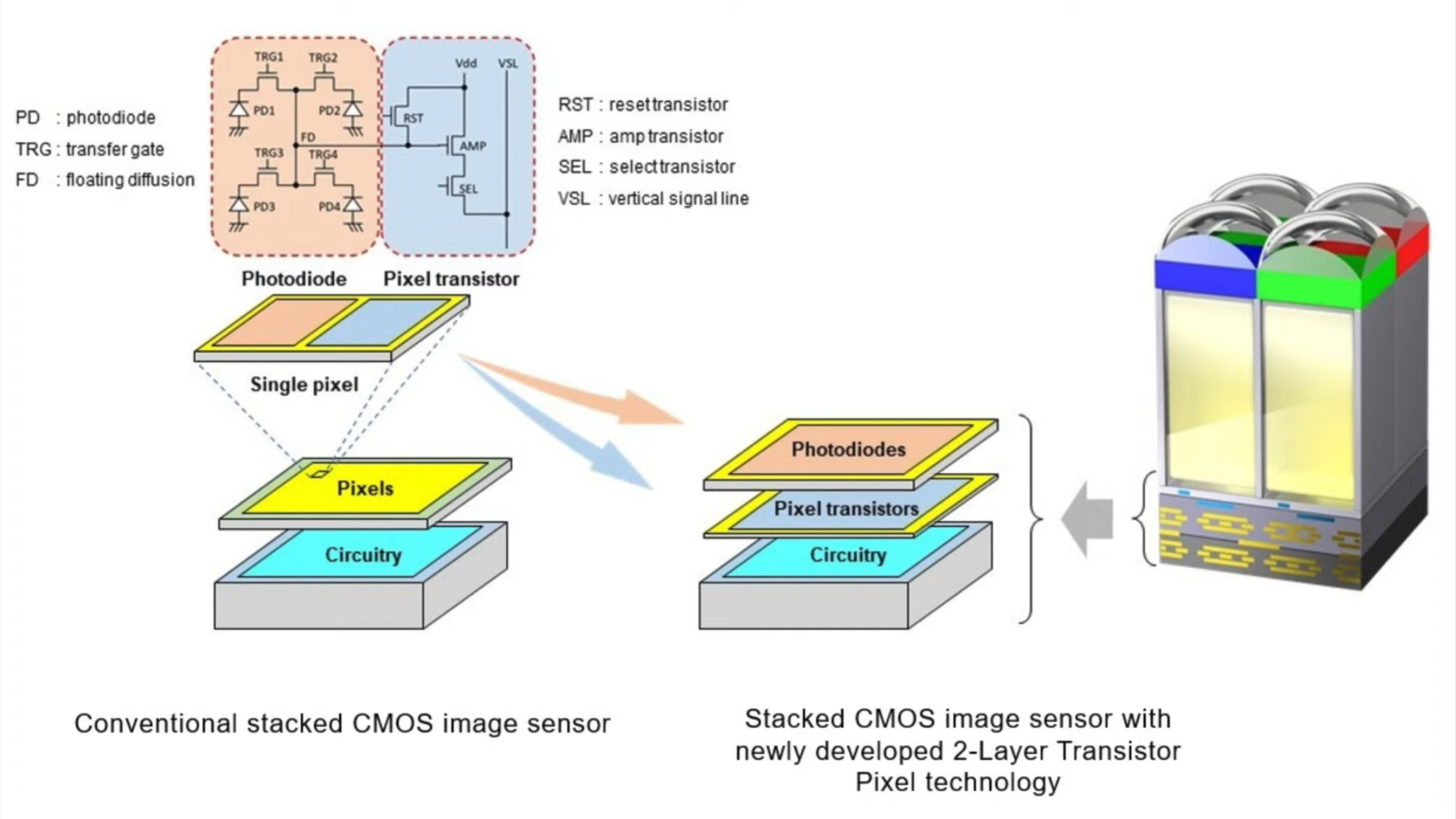
The key difference of this new sensor design is it is said to separate the transistor element of each photosite ('pixel') from the light-sensitive photodiode element, positioning these two elements onto separate stacked layers - the transistors moved beneath the photodiodes. Contrast this with a conventional CMOS sensor where these two elements are positioned next to each other on the same layer, with the transistors consuming roughly half the surface area.
Article continues belowTheory would therefore suggest that being able to utilize the entire sensor area for light-gathering photodiodes could double the sensor's light sensitivity, thereby increasing dynamic range and reducing image noise at high sensitivity. Sony itself states the 2-layer CMOS construction approximately "doubles the saturation signal level".
This dual-layer design, though similar in naming to existing stacked CMOS sensor tech, is very different. Stacked CMOS sensors use the same photodiode layer as conventional CMOS sensors, but add a layer of DRAM to the sensor construction to speed up image readout speed. One main benefit being faster image processing and burst shooting frame rates.
Though seemingly an obvious solution to increase sensor performance, it is apparently very difficult to mass produce dual-layer sensors, hence why we are only just seeing the technology make its way into the consumer market. Stacking the photodiode atop its transistor is said to require extreme alignment precision, along with a bonding temperature far higher than that used in the construction of normal CMOS sensors.
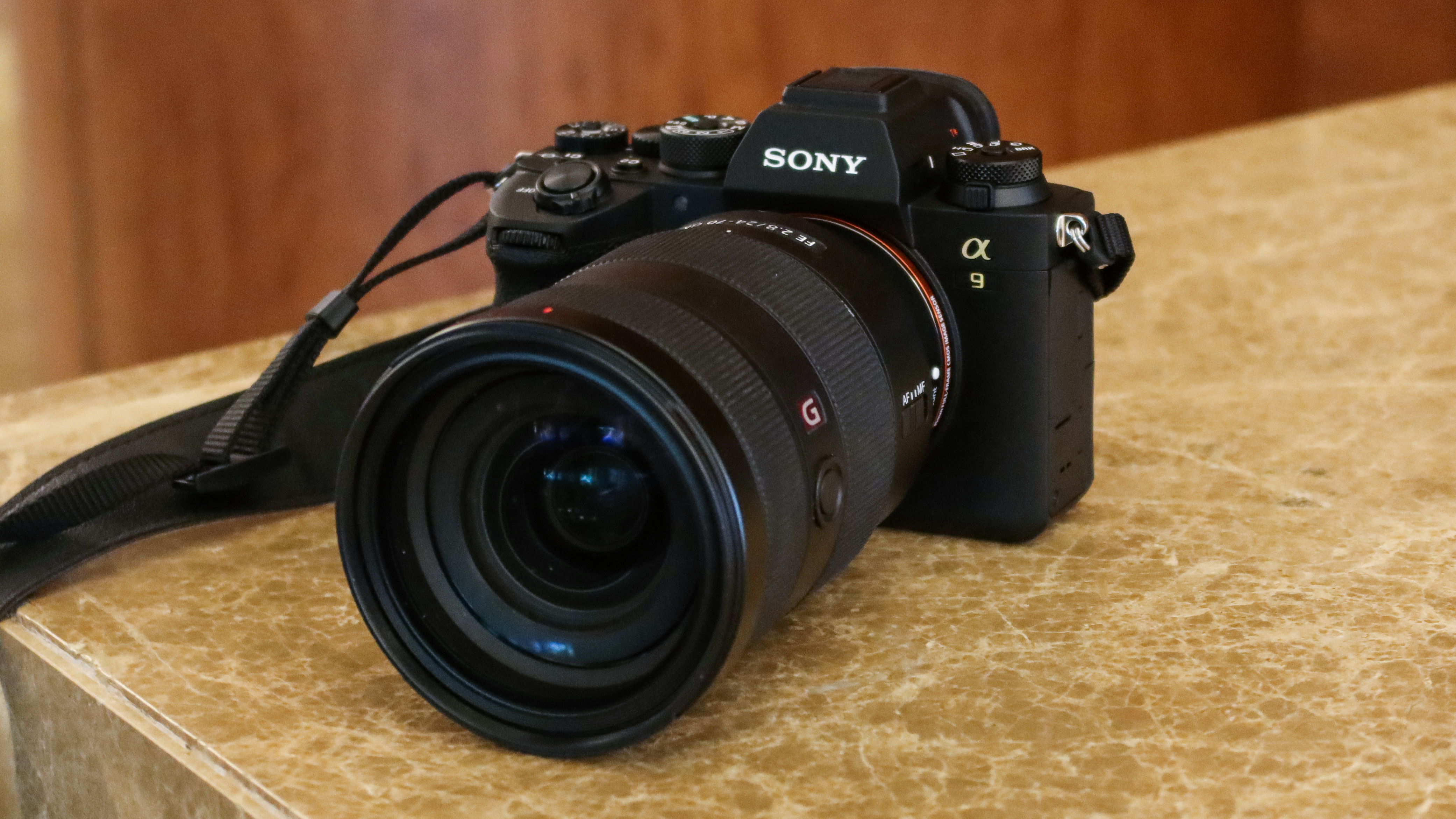
Whether the physical doubling of light-sensitive sensor area then translates to a 2x increase in measurable image quality remains to be seen, but such a best-case scenario seems doubtful. If it were to be true, we could end up with the image quality of a full-frame sensor matching that of today's medium-format sensors. You might also wonder why Sony is debuting this potentially game-changing sensor tech in a camera phone and not a potential new flagship camera like an a9 III or a1 II. If we were to speculate, given the stated technical challenges producing a dual-layer sensor, it's possible current manufacturing processes are simply only able to produce physically small sensor chips. Scaling the technology up to full-frame sensor size could well require more time.
The best camera deals, reviews, product advice, and unmissable photography news, direct to your inbox!
Story credit: Andrea Pizzini Photography, via Sony Alpha Rumors
Read more:
Best Sony phones
The best camera phones
The best burner phones
Which is the best iPhone for photography?
The best TikTok lights
Best camera for TikTok
Ben is the Imaging Labs manager, responsible for all the testing on Digital Camera World and across the entire photography portfolio at Future. Whether he's in the lab testing the sharpness of new lenses, the resolution of the latest image sensors, the zoom range of monster bridge cameras or even the latest camera phones, Ben is our go-to guy for technical insight. He's also the team's man-at-arms when it comes to camera bags, filters, memory cards, and all manner of camera accessories – his lab is a bit like the Batcave of photography! With years of experience trialling and testing kit, he's a human encyclopedia of benchmarks when it comes to recommending the best buys.


